
We the undersigned had certified and acknowledge the successful completion of the Project Report entitled ” ELECTRONIC SIREN”
We certify that we have examined and recommended to Government Technological College for Under-Graduate studies for acceptance the project entitled “ELECTRONIC SIREN” submitted by in partial fulfillment of the requirements for the Diploma of Engineering.
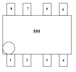
The 555 IC Circuit
The 555 monolatic integrated circuit timer was first introduced by Signetis Corporation in 1927 u8sing bipolar technology. It quickly became an industry strand for, timing and oscillation functions. Many Manufactures produce a version of a 555 IC, some in the CMOS technology. The 555 is a general-purpose IC that can be used for precision timing, pulse generation, sequential timing, time delay generation. The 555 can operate in both astable and monostable modes, with timing pulse ranging from microseconds to hours. It also has an adjustable duty cycle and can generally source or sink output currents up to 200m.
Basic Operation
The basic block diagram of the 555 IC is shown in Fig. The circuit consists of two comparators which drive an RS flip-flop, an output buffer, and a transistor that
discharges an external timing capacitor. The actual circuit of an LM555 timer is also shown.
The RS flip-flop is a digital circuit that will be considered in a later chapter. Here, we will only describe the basic digital function of the flip-input with voltage references set at (2\3)V by the voltage divider comparator output goes high, producing a high output at flip-flop terminated Q. This turns the discharge transistor on and an external timing capacitor starts to discharge.
The output state of the 555 IC is driven by output Q of the RS flip-flop. This output is usually a totem-pole circuit, or a simple buffer, and is generally capable of sourcing or sinking 200mA.
An external reset input to the RS flip-flop overrides all other inputs and is used to initiate a new timing cycle by turning the discharge transistor on.
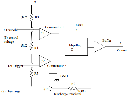
Fig. Basic Block Diagram 555 IC Timer Circuit Diagram, LM555 Timer Circuit
RESISTER
A component is used for its resistance. In the past, most resistors were manufactured from carbon composition, a baked mixture of graphite and clay. These have been almost completely superseded by carbon or metal film resistor. Wire-wound resistors are used for comparatively low values of resistance where the precise value is important, or for high dissipation. They are unsuitable for RF use because of their reactance.
CAPACITOR
A passive circuit component is a capacitance. A capacitor is formed from a pair of conducting surfaces separated by a layer of insulator. A capacitor made from a pair of parallel conducting plates of area S separated by a distance d, with the gap between the plates filled by a dielectric of relative permittivity E, will have a capacitance C given by
C = εrεoS d
where εo is the permittivity of free space.
A component that converts an electrical signal into light signal can be injected into the Fiber.
TRANSISTOR
![]()
The bipolar junction transistor (BJT) is constructed with doped semiconductor regions separated by two PN junctions. The three region is called emitter, base, and collector. The physical representation of the two types of bipolar transistors are shown in Fig; One type consists of two n regions separated by a p region (PNP)and the other consists of two p regions separated by an n region (PNP).
The PN junction joining the base region and the emitter region is called the base-emitter region. The junction joining the base region and the collector region is called the base-collector junction.
Fig. Standard Bipolar Junction Transistor (BJT) Symbols
![]()
Fig. Forward Reverse Bipolar Transistor
The directions of the current in on NPN transistors are as shown in Fig; These diagrams show that the emitter current (IE); the same of the collector current (IC)and the base current (IB).
RECTIFIER
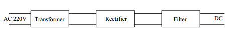
Fig. Block Diagram of Rectifier Circuit
The power supply consists of a transformer, receiver, and filter circuit. The transformer is probably one of the most useful electric devices. The transformer provides a simple means of changing an ac voltage or current from one value to another. A simple transformer consists of two coils (windings). The coil connected to the source is called primary winding and the other one is called the secondary winding. The coils are insulated from each other and from the core.
If a transformer receives energy at a low voltage and delivers it at a higher voltage, it is called step up transformer. When a transformer is supplied some lower voltage, it is called a step-down transformer. We used a step-down transformer in the circuit.
For an autotransformer, the secondary winding is actually part of the primary winding. The rectifier circuit is the process of converting an alternating (ac) voltage into one, that is limited to one polarity.
Rectifier circuit that contains diode is called rectifier diode. The diode can pass current easily in one direction only.
Rectifier diode can be used to charge a RESERVOIR CAPACITOR in order to obtain smooth DC. The rectifier circuit is classified as half-wave and full-wave rectifier.
The output voltage appears only during the positive cycle of the input signal, the circuit is called a half-wave rectifier.
A rectifier output voltage occurs during both the positive and negative cycles of the input signal, this circuit is called a full-wave rectifier.
Full-wave rectifier consists of
(a) Central-tapped full-wave rectifier; and
(b) Bridge full-wave rectifier.
We used Bridge full-wave rectifier.

Fig. Schematic Circuit Diagram of Rectifier
Filter circuit provides a constant voltage to a load. The capacitor used in the filter circuit.
DIODE
The diode can be made of either two of semiconductor materials, silicon, and germanium. Power diodes are usually constructed using silicon and germanium. Silicon diode can operate at higher current and at higher junction temperature, and they have greater reverse resistance.
The structure of a semiconductor diode and it symbol are shown in Figure. The diode has two terminals, an anode, A terminal ( P junction ) and a cathode K terminal ( N junction ). When the anode voltage is more positive than the cathode, the diode is said to be forward biased and it conducts current readily with a relatively low voltage drop. When the cathode voltage is more positive than the anode, the diode is said to be reverse biased, and it blocks current flow. The arrow on the diode symbol shows the direction of convection current flow when the diode conducts.
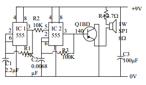
CIRCUIT OPERATION OF ELECTRONIC SIREN
The electronic siren using op-amp 555IC is shown in Fig.This circuit can be used for calling Bell or the emergency etc.
IC1 produce the low-frequency square wave pulses that can be used as the oscillator and IC2 also work for the high-frequency oscillator. The 5th supplied node of IC2 is connected at the end of IC1 output by connecting R2.At low state IC1 output reach 0V and the ground will be simultaneously cut off. In this way, the output signal (high frequency) of IC2 will cause the sound that is simultaneously cut off. The output signal of IC2 will increase by transistor Q2.
By changing the value of R3 and C2 it can be used as the siren of the ambulance and the police cars.
REFERENCES
- Electronic Project 1
- Electronic Project 2
- Devices (Fourth Edition)
- Power Electronic